PCB Making

JVElaser can open standard Gerber files (usually *.gtl, *.gbl, *.cmp, *.sol, *.top, *.bot for the copper layer and *.gtp, *.gbp for the solder paste stencil layer). These files can be used to create PCBs and stencils.

Opening a Gerber File

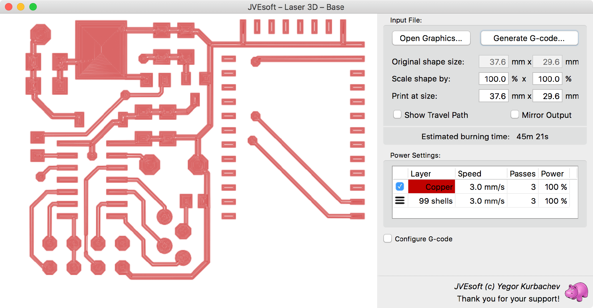
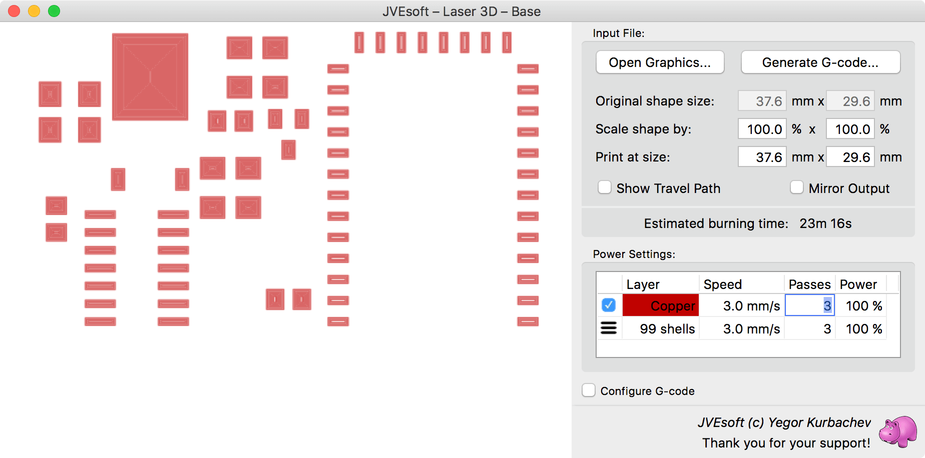
When you choose to open a Gerber file (usually created by a PCB design software, like AutoDesk Eagle), an additional dialog will be opened, allowing you to select how the board layout is being generated.

The following board layout options are supported:

Read from ... Gerber file:

Board shape is taken from another Gerber file, serving as a mechanical layer (usually a *.gml file).

Create ... by offsetting:

Board is considered to be slightly larger than the copper area.

Don’t add any additional layers:

Create only one layer for the Gerber itself (useful for producing solder paste stencils).

Steps

Follow the steps below to create a simple homebrew PCB:

Follow the steps below to create a simple homebrew PCB:

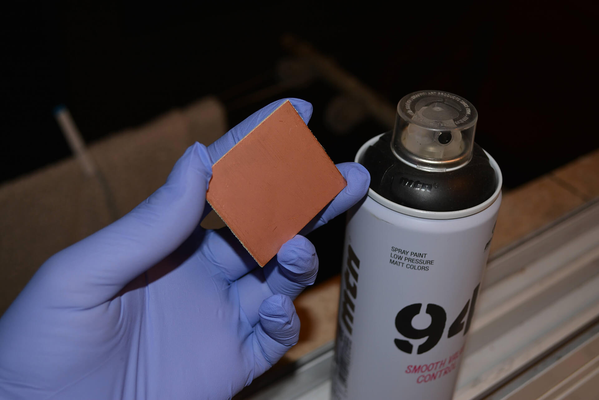
1. Prepare a copper clad PCB and cut it to the required size; washing it beforehand gives the best result.

2. Spray paint it with a thin layer of black matte paint.

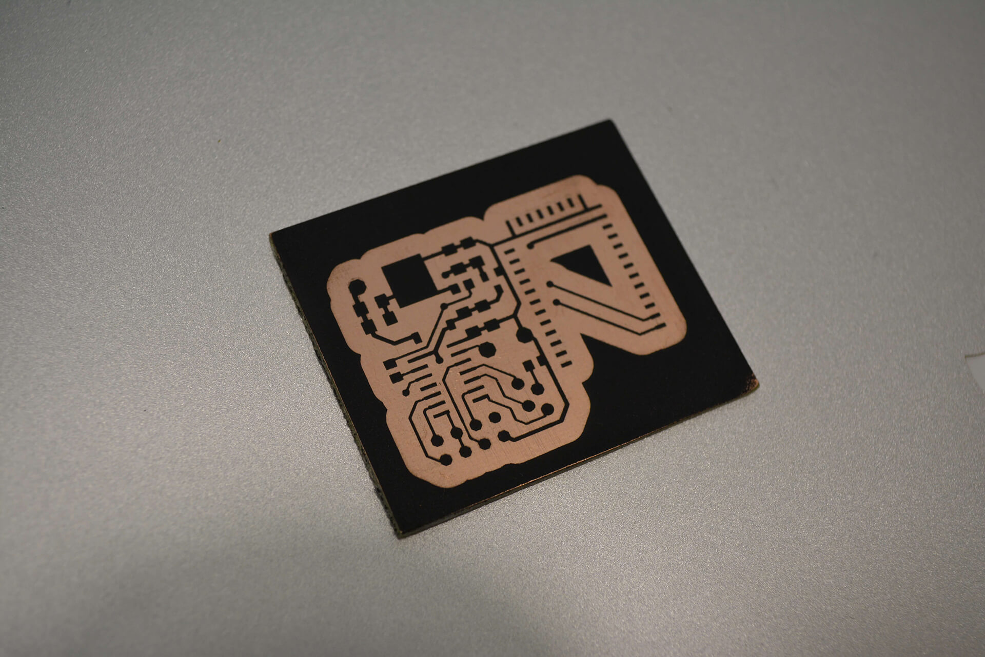
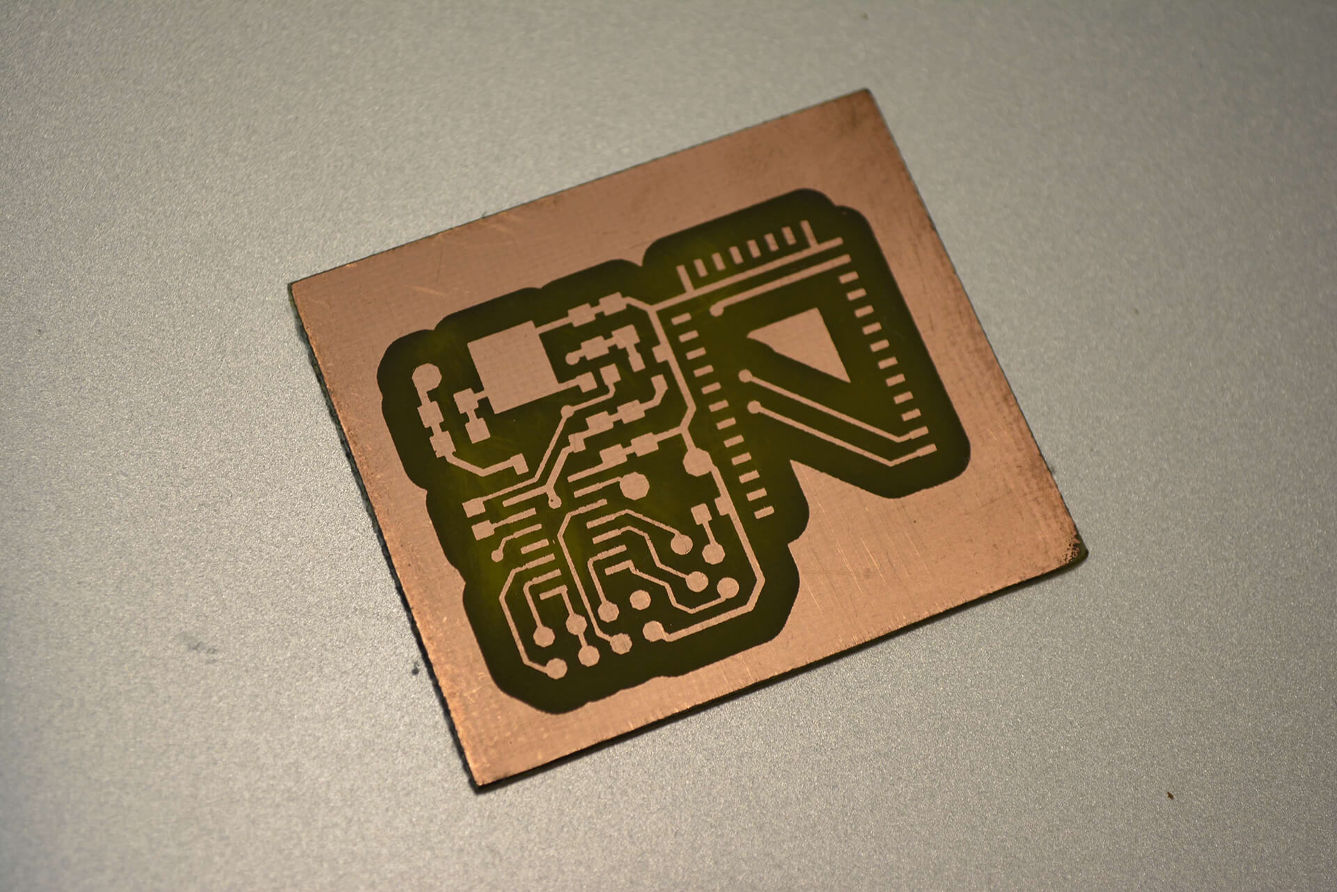
3. Burn the copper mask into the spray paint; best results are achieved if a couple of slow passes are made.

4. After burning the board is covered with the paint residue.

5. Wash the board (with soap or magic sponge).

6. If holes are to be drilled in the PCB, this is the step to do this: drilling after etching might rip the copper, which is more fragile after etching.

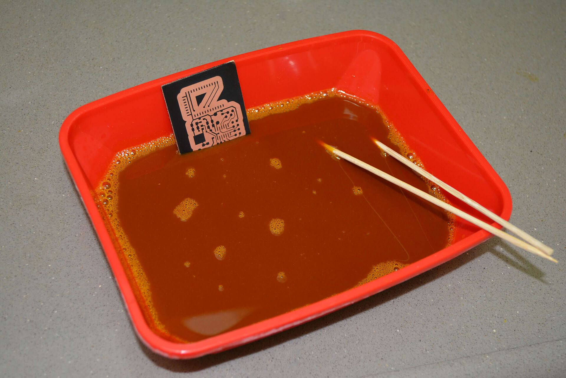
7. Prepare an etching solution and etch until all the exposed copper is gone.

8. When done, clean the board thoroughly to remove the etching solution.

9. Use acetone (or a nail polish remover) to remove the layer of the spray paint.

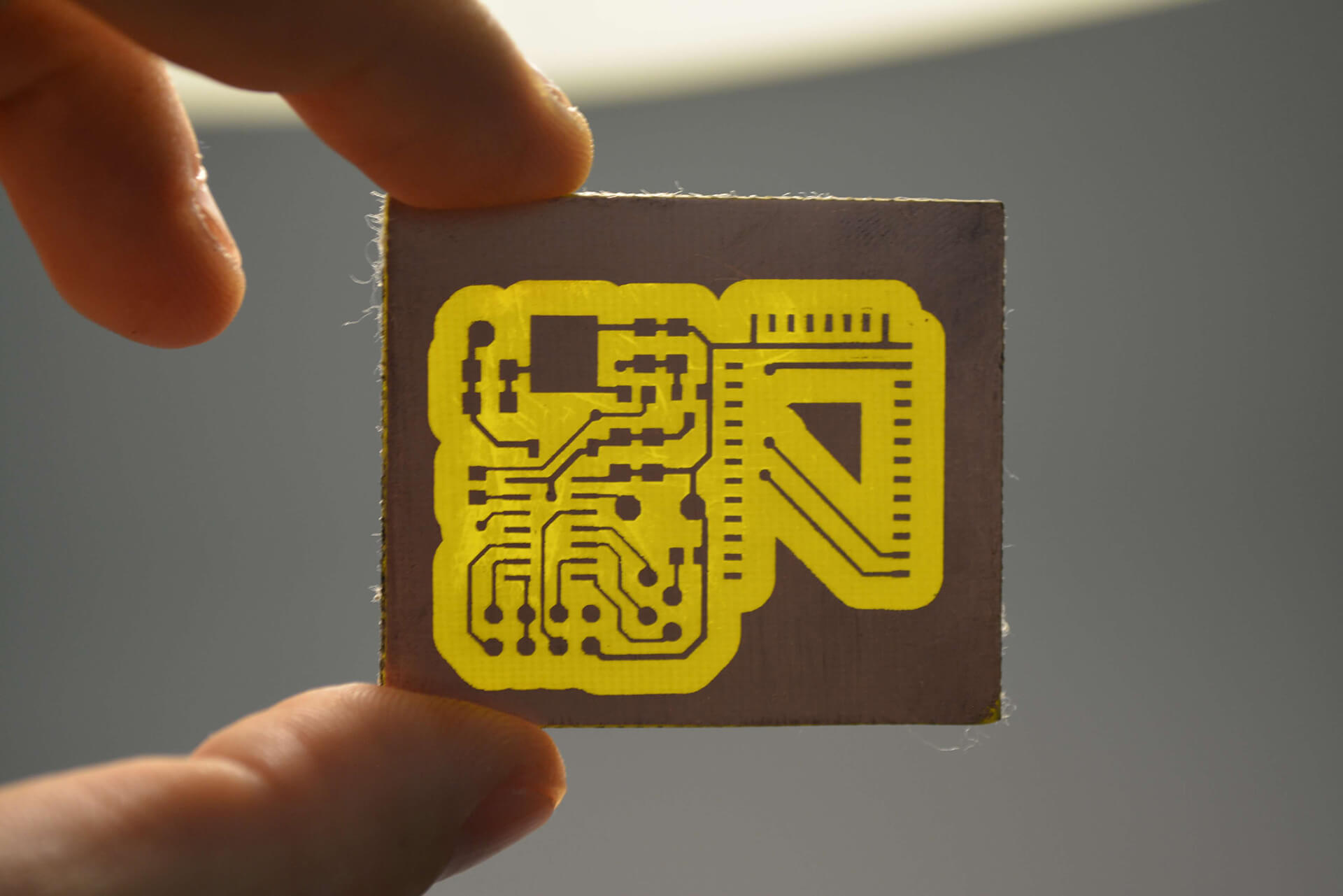
10. The board is ready; fully etched, the entire board except the traces, should be translucent.

11. While we are not doing stencil cutting example here, the process is similar, simply basing this on a sheet of copper, instead of a copper clad board (note, etching will take longer).

Supplies

The two things you’ll need to create PCBs at home are readily available. Copper clad boards are available in a variety of sizes, as single sided or double sided, see examples below (we advice you to buy double sided boards: if you don’t need the other side, the unneeded copper will simply be etched away, but if you do, it’s there for you. Also, there is usually less diversity in single sided items for sale and they are not significantly cheaper):

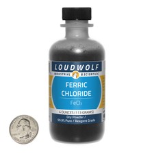
As an etching agent you can use Ferric Chloride or, a more environmentally friendly, Sodium Persulfate.

Note: we are not affiliated with any of these sellers and the references are provided solely as an example; prices are correct as of writing.